A HI-FI VACUUM TUBE AMPLIFIER
by Fred Nachbaur, Dogstar Music © 2002
LTP/CCS Driver Improvement (Sept. 2002)
A: Background
The direct-coupled "long-tail pair" differential amplifier (LTP), driven by a pentode
used as a constant-current source (CCS) is perhaps one of the most accurate phase-splitter
topologies available. However, as implemented in the original RA-100 design it can be quite
touchy to adjust. Furthermore, it can drift with time and temperature, and while the drift is
usually not severe enough to cause any difficulties, it's been a bit of thorn in my side. The
most annoying aspect is that there seems to be no one thing that can be blamed; rather, it seems
to be the result of miniscule drifts in values of virtually all of the components in the circuit,
including the tubes; some specimens seem less stable than others.
The situation can be vastly improved by changing one resistor, and adding three more. As a bonus,
the modification greatly improves the common-mode rejection ratio (CMRR) of the circuit, reducing
the effect of the not-quite-ideal constant-current source.
In the discussions that follow, part numbers refer to the left channel. The right channel
will of course be identical.
B: The Modification
If you've already built up this circuit, modifying it for the new improvements is very simple:
- Cut the connection between the control grid of the 6CB6 constant-current source pentode
(V8 pin 1) and the wiper of the RV503 bias pot.
- Bridge the connection with a 47k resistor, R1001.
- Connect 4.7 megohm resistors (R1001, R1002) between the plates of the LTP triode sections
(pins 1 and 6, V7) and the grid of V8 (pin 1).
- Change R511 from 22 ohms to 1.8k.
If you're building this amplifier from scratch, it's recommended that you include this
modification from the start. The new schematic diagram is shown below.
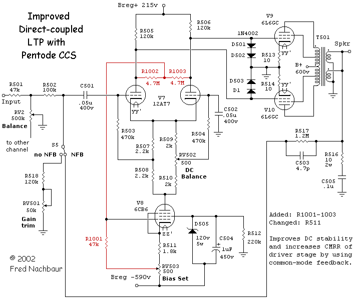
Improving DC stability and CMRR
C: How It Works
The theory is almost absurdly simple. Negative feedback is applied for common-mode signals
via the split voltage-divider consisting of R1001, R1002 and R1003, from the anodes of the
LTP to the control grid of the CCS. In order to accomodate the increased (more positive)
voltage on the CCS grid, its cathode resistance is increased; this introduces a second
source of common-mode negative feedback.
Since the "bias" pot RV503 is inside the feedback loop, its setting will be a lot less
touchy than before. With the values shown, however, it will still have plenty of adjustment
range to accomodate reasonably matched LTP triode pairs and output tube pairs.
The DC Balance adjustment (RV502) is unaffected by this change, since it represents a
differential term. Whatever current is robbed by one half of the LTP is absorbed by the other,
so the common-mode feedback loop never even sees the change.
D: Analysis
Feedback systems can be a nuisance to analyze, since the output affects the input. One method
of analysis involves solving simultaneous equations; an alternate method often used by hobbyists
is iteration (calculating over and over until the results converge). However, my preferred method
is to think inductively, from effect (output) to cause (input). In this circuit, the most
critical voltage is the CCS control-grid voltage, relative to ground (or negative supply, since
it's well-regulated for DC and bypassed for AC). Since we're working in common mode, imagine that
the two triodes are in parallel. This means that the plate load resistors are also effectively in
parallel, with a value of 60k. The voltage on the single anode will be our "output"
signal. Similarly, our feedback resistors are effectively in parallel, for a value of 2.35
megohms. The feedback divider ratio is therefore 50:1.
Let's start by analyzing the circuit as it was before, and ignore the effect of the small
cathode resistor. We'll find the input voltage change required to effect an arbitrary (let's pick
10 volts) output change. The transconductance of the 6CB6 is 8000 µmhos, or 8.0 mA/V. A
ten volt change at the bottom of the combined load resistor (60k) implies a current change of
(10/60) = 0.1667 mA. So the input change required would be only (0.1667/8) = 20.3 millivolts.
In practise, it's not quite as bad as that. There is some cathode feedback due to
the presence of the top portion of the adjustment pot, plus R511 (originally 22 ohms). Let's
assume that this total value is about half of the adjustment, or 250 ohms. The voltage change
developed by our 0.1667 mA error current will therefore be about 41.7 mV. So the required input
change relative to ground or negative supply for a 10 volt common-mode output change will
be (20.3 + 41.7) mV or 62 mV. Better, but still not great. No wonder the circuit's a little touchy!
Now let's look at the modified circuit. The larger value of cathode feedback (1.8k + 250 ohms)
will mean that the drop occasioned by the error current will be (2.05k * 0.1667mA) = 342 mV.
Furthermore, the 50:1 voltage divider from output to input adds (0.02 * 10)V = 200 mV, for a
total of 542 mV. The voltage change relative to ground or negative supply is therefore
(542 + 20.3) mV = 562.3 millivolts. This represents an improvement in DC stability and CMRR of
(562.3 / 62) = 9.1 times better than the original design!
Lower divider ratios could be used for even more common-mode feedback. The cathode resistor R511
would have to be increased to compensate for the additional common-mode grid voltage. There are
some limiting factors, though, which need to be taken into account:
- Adjustment range of the bias pot. You will need to use larger-valued potentiometers if going
much beyond the values given.
- Loading on the output, affecting differential gain. As shown, the feedback networks have
an almost unmeasurable (and certainly inaudible) effect on the overall gain.
- The lower divider element should not be made too high, otherwise grid emission and
electron capture (similar but opposite effects) can come into play. I wouldn't suggest going much
higher than 100k with a high-Gm pentode such as the 6CB6.
- Possible common-mode instability or oscillation due to stray capacitances.
END OF ARTICLE
